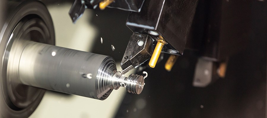
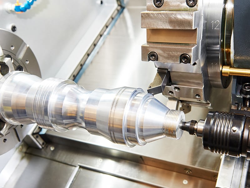
As transistors continue to be miniaturized, the channels through which they conduct current are getting narrower and narrower, requiring the continued use of high electron mobility materials. Two-dimensional materials such as molybdenum disulfide are ideal for high electron mobility, but when interconnected with metal wires, a Schottky barrier is formed at the contact interface, a phenomenon that inhibits charge flow.
In May 2021, a joint research team led by the Massachusetts Institute of Technology and participated by TSMC and others confirmed that the use of semi-metal bismuth combined with the proper arrangement between the two materials can reduce the contact resistance between the wire and the device, thereby eliminating this problem. , helping to achieve the daunting challenges of semiconductors below 1 nanometer.
The MIT team found that combining electrodes with semimetal bismuth on a two-dimensional material can greatly reduce resistance and increase transmission current. TSMC's technical research department then optimized the bismuth deposition process. Finally, the National Taiwan University team used a "helium ion beam lithography system" to successfully reduce the component channel to nanometer size.
After using bismuth as the key structure of the contact electrode, the performance of the two-dimensional material transistor is not only comparable to that of silicon-based semiconductors, but also compatible with the current mainstream silicon-based process technology, which will help to break through the limits of Moore's Law in the future. This technological breakthrough will solve the main problem of two-dimensional semiconductors entering the industry and is an important milestone for integrated circuits to continue to advance in the post-Moore era.
In addition, using computational materials science to develop new algorithms to accelerate the discovery of more new materials is also a hot spot in the current development of materials. For example, in January 2021, the Ames Laboratory of the U.S. Department of Energy published an article on the "Cuckoo Search" algorithm in the journal "Natural Computing Science". This new algorithm can search for high-entropy alloys. time from weeks to seconds. The machine learning algorithm developed by Sandia National Laboratory in the United States is 40,000 times faster than ordinary methods, shortening the design cycle of materials technology by nearly a year. In April 2021, researchers at the University of Liverpool in the United Kingdom developed a robot that can independently design chemical reaction routes within 8 days, complete 688 experiments, and find an efficient catalyst to improve the photocatalytic performance of polymers.
It takes months to do it manually. Osaka University, Japan, using 1,200 photovoltaic cell materials as a training database, studied the relationship between the structure of polymer materials and photoelectric induction through machine learning algorithms, and successfully screened out the structure of compounds with potential applications within 1 minute. Traditional methods require 5 to 6 years.
Post time: Aug-11-2022